

The 2025-2026 period has seen growing industry momentum behind 3D-stacked CPO network switches, with companies increasingly moving away from laterally placed architectures to accommodate AI data center scale-up. In this article, IDTechEx delves into the packaging advancements enabling this transition, and the technological barriers that face the key players driving it.
The power and processing demands of AI infrastructure continue to escalate at a breakneck pace, driving unprecedented east-west (GPU to GPU) traffic to facilitate the parallel computations required for LLM training and inference. As model complexity increases and the worldwide userbase grows, data speed and power efficiency strain against the rapidly approaching limits of today's pluggable-based server rack architectures. To reduce latency and power consumption, and increase bandwidth capacity beyond the pluggable ceiling, optical interconnects must be brought closer to the L2 network switch ASIC (Application-Specific Integrated Circuit) routing traffic both between individual GPUs and throughout the wider server infrastructure.
The most promising solution involves co-packaging the optical engine with the switch electrical integrated circuit (EIC). Expected to drive a bandwidth increase from 51.2 Tbps to 1.6 Pbps within a decade, the transition from pluggable to co-packaged optics is viewed by many as inevitable, and according to IDTechEx's forecast in its updated report on the topic, "Co-Packaged Optics (CPO) 2026-2036: Technologies, Market, and Forecasts", CPO is expected to capture a total market value of US$20B by 2036. But what form will these co-packaged optical and electronic circuits take? In this article, the current and future landscape of network switch design is explored with an eye towards this emergent packaging transition.
Pluggable Transceivers, 2D and 2.5D
In the traditional pluggable model, electrical signals are driven between the ASIC and transceiver optical engine via long copper traces. At today's data rates, copper exhibits low signal integrity, such that a significant proportion of the overall server power draw stems from correction processes at the transceiver.
To mitigate this, initial CPO designs were geared towards reducing this power draw. The EIC and PIC (photonic integrated circuit) were placed side-by-side upon the substrate (2D) or above a connection-rich interposer layer (2.5D), reducing the copper trace length from centimeters to millimeters. These assemblies were the first logical step in improving the performance of network switches beyond pluggable efficiency constraints, but as bandwidth and latency demands grow the optical engine increasingly competes with memory and voltage regulator modules for real estate around the die, necessitating a move towards vertical integration.
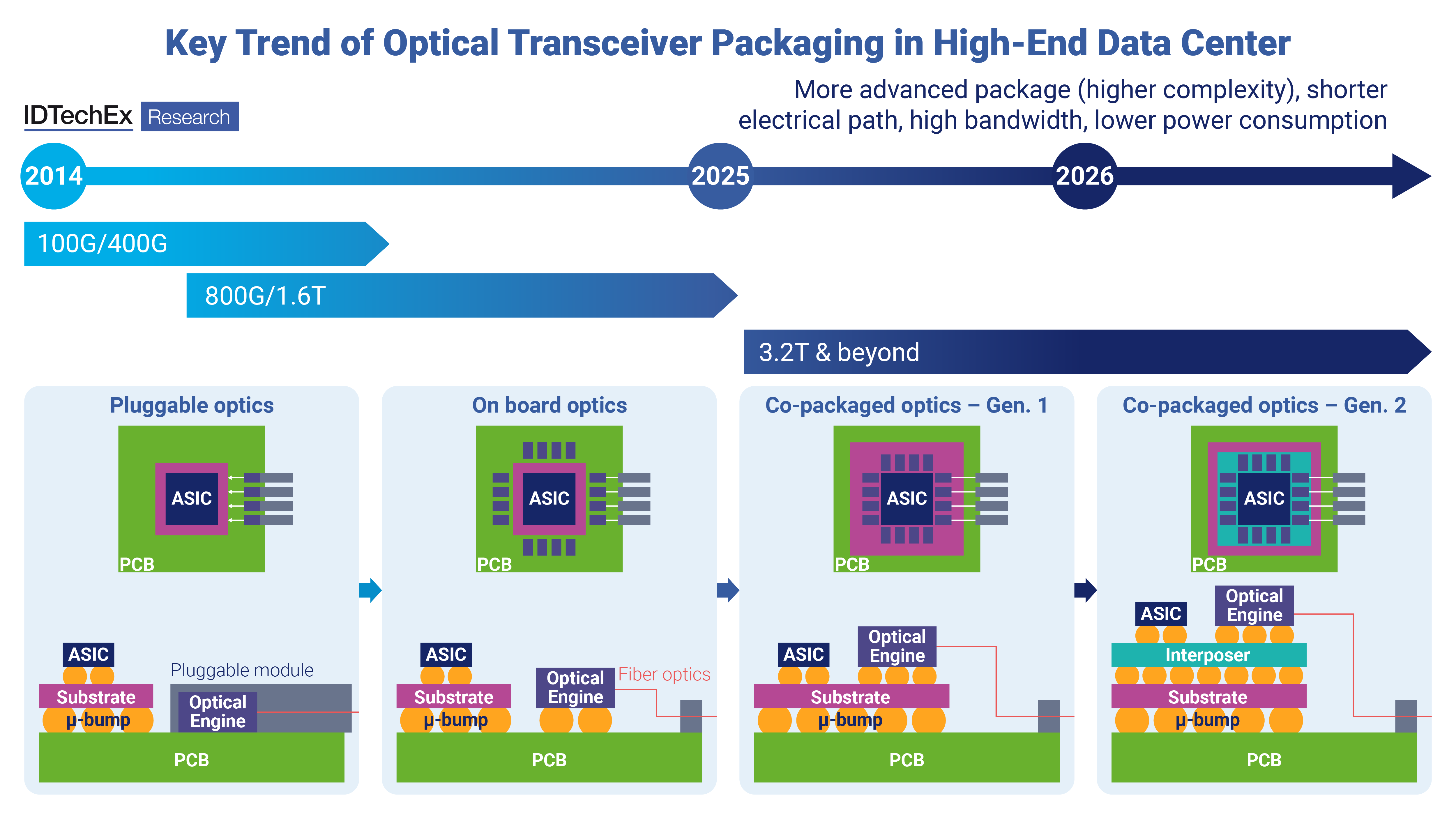
Trends in optical packaging. Image source: IDTechEx
The Advantages and Challenges of 3D Monolithic Packaging
The most direct way to solve this spatial constraint, whilst simultaneously minimizing impedance mismatch and power loss, is to integrate the PIC and EIC into a single die. In this configuration, the close proximity of photonic and electronic components allows for simplified packaging and efficient signal routing.
However, the shared fabrication process struggles with the mismatch in requirements for optimized electronic and photonic circuits. Whereas today's most advanced FinFETs occupy a fabrication node scale of 10 nm or less, photonic components are generally an order of magnitude larger. The fine-pitch, densely packed structures required for high-performance EICs therefore impose constraints on the material stack and layer dimensions which could enhance optical waveguide loss and reduce photodiode performance. Conversely, attempts to optimize the chip towards improved photonic function may lead to transistors with inferior switching and energy-efficiency characteristics. These performance limitations are further compounded by the current reliance of monolithic integration upon 45 and 32 nm CMOS process nodes.
3D Hybrid: A Compromise
Alternatively, 3D hybrid integration offers a means of compromise. By fabricating each integrated circuit separately, the photonic and electronic dies may be finely tuned to their respective carrier before vertical stacking. The complexity therefore shifts to the bonding method itself. To accommodate the dense vertical connections between the EIC and PIC, the interconnect pitch must be continually reduced. However, decreasing pitch places increasingly stringent demands upon alignment and manufacturing yield whilst exacerbating parasitics, pushing widely adopted technologies such as microbumps towards their scaling limits. As explored further in IDTechEx's report on Co-Packaged Optics, Cu-Cu hybrid bonding has emerged as a promising solution offering sub-10 µm pitches, though it suffers from enhanced manufacturing costs.
Whilst the shorter, denser interconnects enabled by Cu-Cu bonding represent a major fabrication advantage, the 3D stacking technique still faces strong barriers impeding its operating performance. In all proposed designs, heat management remains a key issue, but it is at its most difficult within this format where the heat-generating components are concentrated near temperature-sensitive photonic components and the placement of cooling hardware is limited. Today's most advanced co-packaged switches confront this issue by moving the most failure-prone optical component, the laser source, outside of the CPO package. In NVIDIA's Spectrum-X and Quantum-X Photonics platforms, for example, detachable external laser modules maintain separation from the thermal environment of the switch ASIC. This improves module reliability whilst also improving serviceability should these components fail.
IDTechEx Outlook
In the medium term, IDTechEx predicts that the 3D heterogeneous approach to integration will continue to lead the charge, with Cu-Cu hybrid bonding approaches in particular occupying 50% of the total CPO market to balance minimal crosstalk, power consumption and parasitics whilst avoiding the photonic and electronic performance trade-offs inherent to the 3D monolithic structure. The report "Co-Packaged Optics (CPO) 2026-2036: Technologies, Market, and Forecasts" covers these and other trends in CPO packaging alongside detailed analysis of key players within the space.
For more information on this report, including downloadable sample pages, please visit www.IDTechEx.com/CPO, or for the full portfolio of related research available from IDTechEx, see www.IDTechEx.com.
