Designing energy-efficient systems that meet the high bandwidth demands of high-performance computing (HPC) involves key trends in silicon technology: increasing transistor density, enhancing memory capacity, and boosting interconnections between logic ICs and memory. While the demand for more transistors pushes chip design beyond reticle limits—outside the realm of advanced packaging—the other two trends can be effectively addressed through advanced semiconductor packaging techniques.
Enhancing memory capacity can be achieved by integrating high-bandwidth on-chip memory and increasing I/O counts, both made possible by advanced packaging technologies. Similarly, improving interconnections between logic and memory ICs is crucial for system performance, and advanced packaging provides the necessary framework.
Cost management remains a critical focus in this domain. The emergence of chiplet design offers a modular approach to processor development, allowing vendors to optimize cost and performance. By using different process nodes for different components, chiplet design minimizes the reliance on expensive, state-of-the-art nodes for less critical parts, reducing overall costs. Moreover, the need for more I/O is driving the integration of I/O dies within the same module as processing units. Utilizing 2.5D or 3D advanced semiconductor packaging technologies, which enable sub-micron routing, this approach increases I/O counts, boosts memory capacity, and enhances system performance.
Advanced semiconductor packaging trends
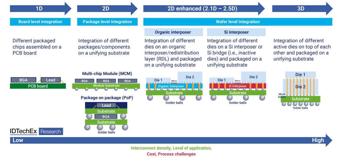
Semiconductor packaging technologies have advanced from basic 1D PCB levels to advanced 3D hybrid bonding at the wafer level, enabling ultra-fine interconnecting pitches and bandwidths exceeding 1000 GB/s with high energy efficiency. This evolution is driven by four key factors: improving power efficiency through innovative designs, boosting performance by increasing I/O points and reducing interconnection length, optimizing area by balancing larger packaging for high-performance computing with compact 3D integration, and reducing costs through the continuous hunt for more affordable materials and enhanced manufacturing efficiency.

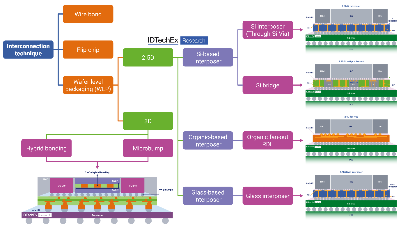
Figure 1. Evolution roadmap of semiconductor packaging.  Figure 2. Overview of advanced semiconductor packaging technologies, categorized by different interconnection techniques.
 Figure 2. Overview of advanced semiconductor packaging technologies, categorized by different interconnection techniques.
 2.5D and 3D packaging technologies are considered to be at the forefront of advanced semiconductor technologies. The advantages and drawbacks of each packaging type in both 2.5D and 3D configurations are outlined below, based on insights from IDTechEx's research reports: "Advanced Semiconductor Packaging 2024-2034: Forecasts, Technologies, Applications" and "Materials and Processing for Advanced Semiconductor Packaging 2024-2034."
2.5D packaging
2.5D packaging involves the use of interposers to connect different chiplets (dies) horizontally on the same package. There are three main types of interposers:
- Silicon (Si) Interposers: These interposers are currently the mainstream in HPC due to their ability to support the finest routing features, allowing for high-performance integration. However, the high costs of materials, high standard manufacturing, and limitations in the packaging area present challenges. To mitigate these, localized Si bridges, which strategically use Si only where necessary, are gaining traction. This method helps overcome area limitations, especially beyond the 4x or 5x reticle limit.
- Organic Interposers: Organic interposers, which use fan-out molding compounds, are considered a cost-effective silicon alternative. Not only are the materials and manufacturing processes cheaper, but scaling up to panel-level packaging (e.g. FOPLP - Fan Out Panel Level Packaging) can further reduce costs. Traditional silicon wafers have a utilization rate of less than 85%, while panels exceed 95%. A 600×600 mm panel offers more than 5 times the effective area of a 300 mm silicon wafer, potentially lowering overall costs by more than 60%. This increase in area utilization leads to higher production capacity, greater design flexibility for AI chips, and substantial cost reductions. Additionally, these materials can be engineered with a lower dielectric constant, reducing resistance-capacitance (RC) delay and improving performance, though achieving the fine interconnect features possible with silicon-based interposers remains challenging.
- Glass Interposers: Glass has become an attractive option due to its tunable coefficient of thermal expansion (CTE), high dimensional stability, and smooth surface, which are ideal for fine routing. Additionally, glass enables panel-level packaging, which significantly reduces costs. Despite these advantages, the ecosystem for glass interposers is still maturing, and large-scale production capabilities are currently limited. However, as these challenges are addressed, glass is expected to play a more significant role in semiconductor packaging.
3D packaging
3D packaging involves stacking chips vertically, which allows for more compact and efficient designs. Two key technologies here are:
- Microbump Technology: This long-established method uses thermal compression bonding (TCB) to create vertical interconnects between stacked chips. While microbump technology is scalable, reducing the bump pitch (distance between bumps) to single digit micrometer leads to challenges like increased formation of intermetallic compounds (IMCs), which can degrade conductivity and mechanical properties. The risk of solder ball bridging also rises, potentially leading to chip failure.
- Hybrid Bonding: This advanced technique creates permanent connections by combining dielectric materials with embedded metal, typically copper (Cu-Cu bonding). Hybrid bonding achieves very fine pitch dimensions, often below 10 micrometers, leading to significant benefits such as higher I/O counts, improved bandwidth, better power efficiency, and reduced parasitic effects. However, the complexity and cost of manufacturing remain significant challenges. TSMC is the leading provider of 3D hybrid bonding technology, which is currently utilized in several high-end server products, including select AMD Instinct™ and EPYC models.
Dielectric material for 2.5D and 3D packaging
In 2.5D semiconductor packaging, achieving high bandwidth depends on the redistribution layer (RDL), which includes crucial features like line/space dimensions, via sizes, and pad layout. Traditional inorganic dielectrics like SiO2 can achieve fine line/space features but are hindered by high dielectric constants (Dk=3.9) and are costly due to their association with silicon manufacturing techniques. This impairs high-speed communication and increases costs.
Organic dielectric materials are being explored as viable alternatives due to their lower dielectric constants and cost benefits. However, choosing the right organic dielectrics involves balancing several factors, as highlighted in IDTechEx's "Materials and Processing for Advanced Semiconductor Packaging 2024-2034" report. Key parameters include dielectric constant (Dk), loss tangent (Df), coefficient of thermal expansion (CTE), elongation to failure, Young's modulus, and moisture absorption. Ideally, materials should have low Dk and Df, a CTE compatible with silicon and copper, high elongation for flexibility, and a moderate Young's modulus for stability. However, selecting materials often requires trade-offs; for instance, polymers with low Dk may have higher CTE, which can affect device reliability and packaging design. Balancing these parameters is crucial for optimizing material performance in semiconductor packaging.
In 3D semiconductor packaging, hybrid bonding now employs inorganic dielectrics like SiO2 or SiCN, which face difficulties with manufacturing challenges in fine-scale patterning and demand advanced front-end manufacturing techniques. Organic dielectrics, similar to those used in 2.5D packaging, offer benefits such as lower dielectric constants, reduced RC delay, and improved defect tolerance. They also potentially allow for back-end manufacturing techniques, which could lower production barriers, enable more industry players to participate, enhance the ecosystem, and reduce costs. However, the use of organic dielectrics in 3D hybrid bonding is still under development due to challenges like high bonding temperatures and compatibility with chemical mechanical planarization (CMP). High temperatures can affect sensitive materials, and differences in modulus between copper and polymers complicate the bonding process. Despite these challenges, it remains a promising area of research for enhancing 3D packaging technology.
Co-Packaged Optics
Optical interconnects are crucial for next-generation high-end data centers because they can overcome the I/O bottleneck that limits data transfer speeds. Optical interconnects use light instead of electricity to leverage photons, which experience no resistance and can travel long distances with minimal loss. This enables much higher bandwidth and faster data transmission between chips and chiplets than traditional electrical methods. As data centers demand ever-increasing speeds and efficiencies, optical interconnects facilitate rapid, high-capacity communication, addressing critical performance and scalability challenges and ensuring that hardware can effectively meet the growing data demands.

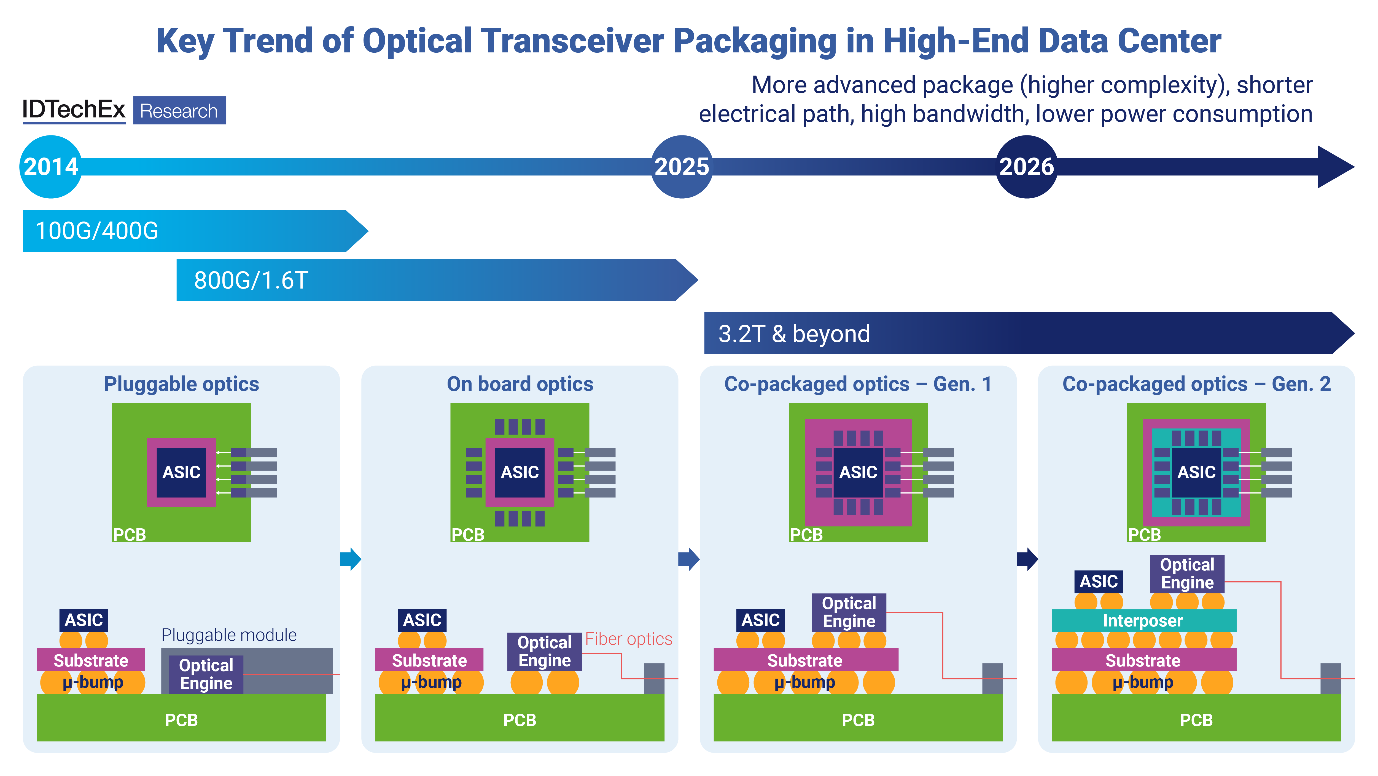
Figure 3. Key trend of optical transceiver in high-end data center.
The transition from pluggable optical transceivers, the incumbent optical transceiver technology in high-end data centers, to co-packaged optics (CPO) is driven by the need to address signal integrity and integration density limitations. Pluggable optics struggle with high power consumption and signal integrity issues due to increasing data rates and connector densities. In contrast, CPO integrates optical modules directly onto the switch ASIC, reducing electrical distances and improving signal integrity. This approach enhances performance, supports higher-speed data transmission, and overcomes the constraints of traditional pluggable modules, optimizing communication data rates per lane.
Advanced semiconductor packaging is a critical enabler for Co-Packaged Optics (CPO). For example, ways to integrate photonic ICs (PIC) and electronic ICs (EIC) influence bandwidth density and packaging parasitics. 3D monolithic integration offers minimal parasitics but uses older CMOS nodes for EIC, affecting performance and energy consumption. 2D integration offers the lowest cost but suffers from significant parasitics and reduced bandwidth and is, therefore, unsuitable for CPO. 2.5D integration provides a balance with manageable parasitics and cost but is less efficient than 3D hybrid solutions. 3D hybrid integration, using techniques like TSV in active interposers, Cu-Cu bonding, minimizes parasitics and provides the best performance, though it faces thermal management challenges. A more in-depth discussion about CPO packaging can be found in IDTechEx recent report "Co-Packaged Optics (CPO) 2025-2035: Technologies, Market, and Forecasts".
Outlook
Advanced semiconductor packaging is experiencing significant growth due to the interplay of technological, economic, and market forces. As silicon scaling approaches its limits, advanced packaging offers a viable alternative for boosting chip performance, particularly for high-performance computing (HPC) applications like AI and data centers, which demand increased computational power and bandwidth. This technology facilitates heterogeneous integration of diverse chiplets, addressing the needs for higher bandwidth and improved power efficiency while also providing a cost-effective solution amid rising chip manufacturing costs. Furthermore, the surge in 5G, AI, automotive, and industrial applications, combined with global competition and supply chain dynamics, is accelerating the advancement and adoption of these packaging technologies.
For more detailed insights into advanced semiconductor packaging technologies, explore IDTechEx's comprehensive portfolio, including "Advanced Semiconductor Packaging 2024-2034: Forecasts, Technologies, Applications," "Materials and Processing for Advanced Semiconductor Packaging 2024-2034," and "Co-Packaged Optics (CPO) 2025-2035: Technologies, Market, and Forecasts."
IDTechEx's market research stands out for its in-depth technical analysis, primary data collection, and unbiased appraisals. For the full portfolio of semiconductor-related research, please visit www.IDTechEx.com/Research/Semiconductors.
Technology Innovations Outlook 2025-2035
This article is from "Technology Innovations Outlook 2025-2035", a free collection of insights from industry experts highlighting key technology innovation trends shaping the next decade. You can download the full collection here.
About IDTechEx
IDTechEx provides trusted independent research on emerging technologies and their markets. Since 1999, we have been helping our clients to understand new technologies, their supply chains, market requirements, opportunities and forecasts. For more information, contact research@IDTechEx.com or visit www.IDTechEx.com.


